FPGA Programming with Linux
Free software licenses and operating systems like GNU/Linux make it possible to learn programming and customize state-of-the-art software in countless ways. Hacking software, however, isn't the last frontier anymore. What if you could hack integrated circuits directly—that is, tell a chip to connect its internal transistors to create exactly the custom, real-time digital hardware you want? This is precisely what you can do with Field Programmable Gate Arrays (FPGAs). In this article, I explain how to do it with nothing else but your Linux computer and an inexpensive development board.
This isn't the first time Linux Journal has covered FPGAs (see Resources), but these devices have made huge progress since those articles were written. Plus, prices for powerful development boards have come down dramatically. Today, you can do really cool things with a $200–$300 FPGA-based board, a typical personal computer and one square foot of desk space. Finally, the FPGA community is now big enough and stable enough to make life much easier for beginners. The major FPGA makers offer text or video tutorials and forums where even newbies can find support. Above all, Web sites like Opencores.org codevelop and release Linux-compatible FPGAs and boards like the EUS 100LX with the same spirit (and licenses) as free software. In summary, the barrier to entry is much lower now than it was even just a couple years ago, making FPGA design both a cool hobby and an affordable and interesting addition to the offerings of even high schools.
A digital integrated circuit (IC) is a chip that deals only with binary digits—meaning signals that can assume only one of two states: 0 or 1, high or low voltage and so on. An FPGA is an IC consisting of one array of digital logic gates. These basic circuits, made up of a few transistors each, instantiate either a flip-flop or lookup tables capable of implementing any boolean function of up to four binary signals. The magic of FPGAs is that the connections among the logic gates (the actual circuit you need) are made at power-up by reading the configuration instructions written into a bit file. Changing the file changes the function of the FPGA.
As flexible as they are, microprocessors are always and only microprocessors: single-purpose hardware that is capable only of executing (relatively slowly) instructions in one machine language. An FPGA, instead, becomes whatever hardware you need. It can morph into a microprocessor, a game console, a real-time IP switch or encryption device, an antitheft server or anything else you can imagine. The only limits are that your circuit cannot require more transistors or external pins than those physically present on the chip, and it can't go faster than the intrinsic propagation delay from gate to gate.
That said, modern FPGAs are powerful enough to let you squeeze several Linux-compatible microprocessors, like the Nios, the PowerPC or the Microblaze, inside them and still have lots of room for your own custom circuits. In many cases, you can load certified CPU designs from libraries and place them on silicon with simple commands, creating very flexible, complete systems inside just one chip.
The major manufacturers of FPGAs and other programmable ICs are Altera and Xilinx, followed by Lattice and Atmel. Although the example in this article uses Xilinx products, the general procedure is the same with all vendors, and all of them have similar boards. In all cases, the design software is closed-source and often expensive, but it is possible to download either free trial versions valid for one or two months, or free versions with reduced functionality but free upgrades and no expiration date.
The current way to design FPGAs is to write a behavioral model in a Hardware Description Language (HDL), like Verilog or VHDL, which supports concurrency and synchronous circuits. Concurrency allows you to create fully parallel, independent processes, each describing how to update some variables continuously. Synchronous circuits, instead, are those made of flip-flops that change their state only on the edge of some clock signal.
After the design has been written and verified with an HDL simulator, a compiler creates a list of all the logic gates and the wires (nets) that must connect them to reproduce the functionality of the HDL model. After this logic synthesis, layout programs read the netlist and several constraints files to find out which logic gates inside the FPGAs must be used and which physical, internal wires must connect them to each other. The end result is the bit file that the FPGA reads at power-up.
The official Xilinx design suite is called ISE Foundation (www.xilinx.com/ise), and the reduced functionality version is called Webpack. Both programs run on Windows, Red Hat Enterprise and SUSE Linux Enterprise (32- or 64-bit). Other Linux distributions may work too, but there is no guarantee.
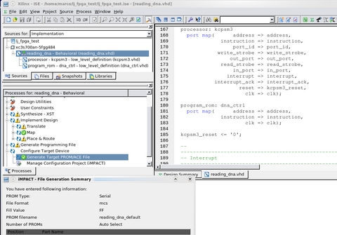
ISE has a graphical installer where you must accept the software license and enter the key you got after a free registration on the Xilinx Web site. After it's finished, you'll find a script called settings32.sh or settings64.sh in the installation directory—that's the one you have to source to add the Xilinx software to your path. After this, type ise at the prompt to launch the Project Navigator (Figure 1). This is a front end to a bunch of specialized programs, one for each design phase. You also can run most of these back-end utilities from the command line. The Navigator includes a Tcl prompt and, if you select Project→Generate Tcl Script, it will save all the commands you entered through the GUI as a Tcl script.
Other ISE components, like the simulator, the FPGA Editor and ChipScope, have graphical interfaces. You'd use the FPGA Editor to place and connect single gates manually when the software fails to do it according to your specs. ChipScope is like a software oscilloscope with a USB probe. During synthesis, you can add special circuits to your design that will buffer the internal signals you want to see and send them over a USB cable to the ChipScope software for display. We'll see the ISE HDL simulator at work in a moment.
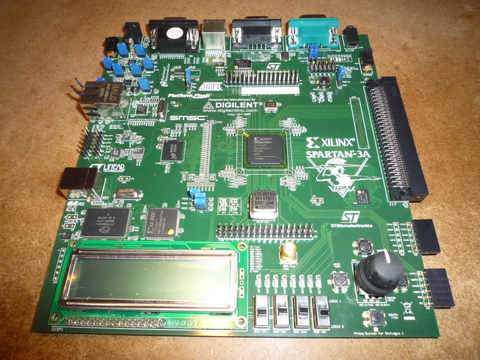
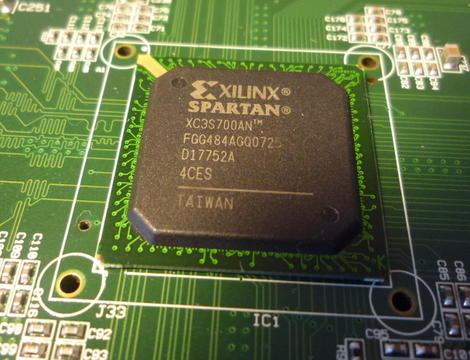
The board I got from Xilinx for this article is the Spartan-3AN Starter Kit (Figure 2), based on the Spartan XC3S700AN FPGA (Figure 3), which contains about 700K system gates. Around it there are several memory chips, a 50MHz onboard clock, a connector for an external clock and several extra components, from D/A and A/D converters to generic I/O pins, assorted LEDs, sliders and push buttons and, finally, a two-line LCD display. The ports (Figure 4), are enough to make a full-custom Linux PC out of this board: 10/100 Ethernet/PHY, USB, keyboard, VGA, serial and stereo mini-jack for PWM audio. A universal power adapter and USB cable are included, as are four different bit files that demonstrate the capabilities of the FPGA. The corresponding design files are freely downloadable from the Xilinx Web site.
In order to show you what it's like to design custom digital hardware and how FPGA development software works, I've modified one of the demo circuits loaded into the Starter Kit, the DNA reader by Xilinx Senior Engineer Ken Chapman.
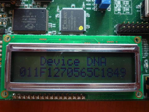
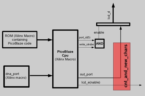
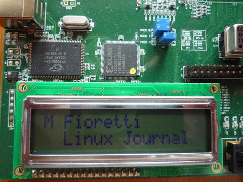
Spartan FPGAs have a unique ID number, called DNA. The DNA reader displays the intro string “DNA Reader by Ken Chapman”, and then this number is displayed on the LCD screen (Figure 5), working as shown in Figure 6. An Xilinx hardware macro called dna_port reads the DNA ID from the silicon. A PicoBlaze processor first displays the intro string, then gets the DNA ID from dna_port and finally sends it, one character at a time, to the LCD interface through the lcd_d data bus. The PicoBlaze code is stored into the dna_ctrl ROM.
My modification consists of a small extra circuit that overwrites the default intro string on the fly with one saying “M Fioretti Linux Journal”. Be warned that this is a hack made only for demo purposes. In the real world, if you actually needed to change that string, it would make much more sense to rewrite the PicoBlaze assembly code. Because this is an article about HDL design in FPGAs, however, I went for a solution based on easy-to-read HDL code whose effect is easily visible in one picture.
My extra circuit is shown in red in Figure 6: a counter and decoder that detect when the PicoBlaze is driving the LCD data port (lcd_d) and send different characters to it. The VHDL source code corresponding to this extra hardware is shown in Listing 1, which is not the complete, working VHDL file I used, but only an excerpt meant to give you an idea of how HDL coding works.
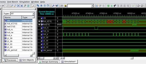
Lines 1–12 define input and output ports of the top-level circuit, the reading_dna module. You must declare all internal registers and wires before using them (lines 17–23). HDLs support hierarchy; you can instantiate other modules by declaring them and connecting all their ports to the right signals (lines 26–49). Line 53 shows a first example of a synchronous process. Depending on the value of the cnt_ops counter, whenever there is a positive edge of the clock (line 56) and the processor sets the signals write_strobe and port_id(6) high, the lcd_output_data register loads the character from the processor or the one from my extra logic (lines 62–68). The cnt_and_new_chars process starting at line 80 does the real work. First, it samples the LCD enable signal to count (line 91) the write accesses to the LCD. One cycle after a write occurs, working with the new counter value (line 99), the process calculates the next current_character that should be displayed. If you look at lines 101–125 you'll see that, instead of the DNA number, the display should show the ASCII string “M Fioretti Linux Journal”. A quick simulation (Figure 7) proves that the new process sends those characters to the display at the right times—that is, when the lcd_rs signal is high (low would indicate LCD configuration commands).
Listing 1. VHDL Source Code
  1	entity reading_dna is
  2	    Port ( led    : out std_logic_vector(7 downto 0);
  3	           lcd_d  : inout std_logic_vector(7 downto 0);
  4	           lcd_rs : out std_logic;
  5	           lcd_rw : out std_logic;
  6	           lcd_e  : out std_logic;
  7	           j2_30  : out std_logic;
  8	           j2_26  : out std_logic;
  9	           j2_22  : out std_logic;
 10	           j2_14  : out std_logic;
 11	           clk    : in std_logic);
 12	    end reading_dna;
 13	--
 14	architecture Behavioral of reading_dna is
 15	--
 16
 17	-- start extra signals for LJ demo
 18	signal   lcd_e_copy        : std_logic;
 19	signal   lcd_e_del_1       : std_logic;
 20	signal   lcd_e_del_2       : std_logic;
 21	signal   current_character : std_logic_vector(7 downto 0);
 22	signal   cnt_ops           : integer range 0 to 49999999 := 0;
 23	-- end extra signals for LJ demo
 24	begin
 25
 26	  device_dna: dna_port
 27	    port map(   din => dna_din,
 28	               read => dna_read,
 29	              shift => dna_shift,
 30	               dout => dna_dout,
 31	                clk => dna_clk);
 32
 33	  processor: kcpsm3
 34	    port map(      address => address,
 35	               instruction => instruction,
 36	                   port_id => port_id,
 37	              write_strobe => write_strobe,
 38	                  out_port => out_port,
 39	               read_strobe => read_strobe,
 40	                   in_port => in_port,
 41	                 interrupt => interrupt,
 42	             interrupt_ack => interrupt_ack,
 43	                     reset => kcpsm3_reset,
 44	                       clk => clk);
 45
 46	  program_rom: dna_ctrl
 47	    port map(      address => address,
 48	               instruction => instruction,
 49	                       clk => clk);
 50
 51	  kcpsm3_reset <= '0';
 52
 53	  output_ports: process(clk)
 54	  begin
 55
 56	    if clk'event and clk='1' then
 57	      if write_strobe='1' then
 58
 59	        -- 8-bit LCD data output address 40 hex.
 60
 61	        if port_id(6)='1' then
 62	          -- lcd_output_data <= out_port;
 63			  --extra code for LJ demo
 64		      if ((cnt_ops >=  8 and cnt_ops <= 17) or
 65		          (cnt_ops >= 19 and cnt_ops <= 32))  then
 66		        lcd_output_data <= current_character;
 67		      else
 68	            lcd_output_data <= out_port;
 69	          end if; --end extra code for LJ demo
 70	        end if;
 71
 72	      end if;
 73
 74	    end if;
 75
 76	  end process output_ports;
 77
 78	  -- LCD interface
 79
 80	  cnt_and_new_chars: process(clk)
 81	  begin
 82	    if clk'event and clk='1' then
 83
 84		  if port_id(5)='1' and write_strobe='1' then
 85		    lcd_e_copy <= out_port(0);
 86		  end if;
 87
 88	      lcd_e_del_1 <= lcd_e_copy;
 89	      lcd_e_del_2 <= lcd_e_del_1;
 90
 91	      if (lcd_e_copy ='1' and lcd_e_del_1='0') then -- posedge
 92	        if cnt_ops=49999999 then                    -- inc counter
 93	          cnt_ops <= 0;
 94	        else
 95	          cnt_ops <= cnt_ops + 1;
 96	        end if; -- if cnt_ops=49999999
 97		  end if; -- end (lcd_e_copy ='1' and lcd_e_del_1='0')
 98
 99	      if (lcd_e_del_1 ='1' and lcd_e_del_2='0') then  -- posedge
100	        case cnt_ops is                -- character generator
101		    when  8 => current_character <= "01001101"; -- M
102		    when  9 => current_character <= "00100000"; -- space
103		    when 10 => current_character <= "01000110"; -- F
104		    when 11 => current_character <= "01101001"; -- i
105		    when 12 => current_character <= "01101111"; -- o
106		    when 13 => current_character <= "01110010"; -- r
107		    when 14 => current_character <= "01100101"; -- e
108		    when 15 => current_character <= "01110100"; -- t
109		    when 16 => current_character <= "01110100"; -- t
110		    when 17 => current_character <= "01101001"; -- i
111
112		    when 19 => current_character <= "01001100"; -- L
113		    when 20 => current_character <= "01101001"; -- i
114		    when 21 => current_character <= "01101110"; -- n
115		    when 22 => current_character <= "01110101"; -- u
116		    when 23 => current_character <= "01111000"; -- x
117		    when 24 => current_character <= "00100000"; -- space
118		    when 25 => current_character <= "01001010"; -- J
119		    when 26 => current_character <= "01101111"; -- o
120		    when 27 => current_character <= "01110101"; -- u
121		    when 28 => current_character <= "01110010"; -- r
122		    when 29 => current_character <= "01101110"; -- n
123		    when 30 => current_character <= "01100001"; -- a
124		    when 31 => current_character <= "01101100"; -- l
125		    when 32 => current_character <= "00100000"; -- space
126
127		    when others => current_character <= "00100000"; -- space
128
129		    end case;
130	      end if; -- end (lcd_e_del_1 ='1' and lcd_e_del_2='0')
131
132
133	    end if; -- clk'event and clk='1'
134	  end process cnt_and_new_chars;
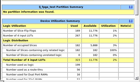
The procedure to transform this really simple HDL model into properly connected gates on silicon is equally simple. Double-click, one at a time, the icons in the left-center pane of the Project Navigator shown in Figure 1: synthesize, Implement Design, Generate Programming File and Configure Target Device. If you clicked directly on the last one, ISE would do all the previous steps in the right order anyway, but doing it in steps is a better way to learn. Eventually, you'll get the bit file and a final report like the one shown in Figure 8, showing how much silicon was used. Remember, what we just did is actual hardware—that is, transistors directly connected to do, in real time, what we ordered them to do. All that remains to make it actually happen is to load the bit file in the FPGA. Figure 9 shows the result.
Due to space constraints, I have given only a very limited view of the FPGA design flow. Pushing FPGAs to the limits requires lots of skill and experience. I have said nothing about floor planning, optimization or simulation strategies, nor have I gone into how to run Linux inside FPGAs. All these are excellent topics for future articles.
My goal with this article was simply to show that it is very easy to start learning these skills, and that there already is a strong community to help you. Students, for example, might consider whether FPGAs are what they need to become the next Linus or Steve Jobs. In my opinion, any high school already teaching programming should add FPGA to its courses. If yours is already doing it, please let me know.
I wish to thank K. Chapman and F. Porpora at Xilinx, and the FPGA Gurus of DekItalia.com, who helped me greatly in preparing this article.
Resources
Xilinx FPGA Design Tools for Linux by Michael Baxter: www.linuxjournal.com/article/6857
Embedded System à la Carte by Michael Baxter: www.linuxjournal.com/article/6073
Spartan Starter Kit Datasheet: www.xilinx.com/products/devkits/HW-SPAR3AN-SK-UNI-G.htm
OpenCore's Linux and Xilinx FPGA Dev Board: www.opencores.org/?do=project&who=eus100lx
Xilinx Linux Forum: forums.xilinx.com/xlnx/board?board.id=ELINUX
Xilinx Documentation: www.xilinx.com/design
Marco (mfioretti.com) is a freelance writer, activist and teacher, concentrating on open digital standards and technologies and their relations and impact on civil rights and education. He's also the author of the Family Guide to Digital Freedom (digifreedom.net).


