Xilinx FPGA Design Tools for Linux
A field programmable gate array (FPGA) is a user-programmable piece of silicon constructed in very large-scale integration (VLSI) technology. The VLSI transistor-level detail is absolutely predefined in an FPGA. Internally, the FPGA consists of a matrix-like fabric of logic and interconnect elements that are inherently flexible. Flexibility is accomplished through programmable SRAM memory cells that define the silicon resources. FPGAs are standard commodity parts with trillions of possible user configurations. This essential organizational structure of the FPGA has persisted through two decades of VLSI technology development. However, today's FPGAs are utterly unlike those of yesteryear.
FPGAs are blurring the lines between hardware and software in systems. FPGA devices are inherently soft-programmable and may be changed dynamically during the operation of a system. More compellingly, FPGA devices now also contain embedded microprocessors within the logic fabric, and these microprocessors can run Linux. Imagine a Linux computer with up to millions of gates of flexible logic immediately around it. One way to grok this new paradigm is to think of the following: “Software is configuration bits for hardware.”
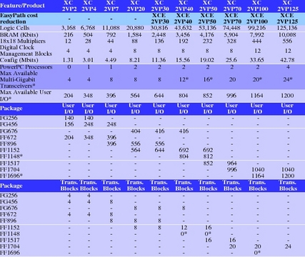
FPGA design is custom silicon design with less effort than full-custom VLSI design. Besides processor cores, FPGAs today not only have logic gates and flip-flops, they also have large Block RAMs, embedded hardware multipliers, arithmetic acceleration logic, digital clock managers (DCMs) for frequency synthesis, multistandard system I/O cells with programmable line termination and multi-gigabit transceivers (MGTs). These system-oriented resources, along with the kinds of device packages and user I/O counts, are enumerated in Figure 1, which shows the most advanced of the FPGA devices, the Xilinx Virtex-II Pro family.
The technology of VLSI memory is everything in this equation—FPGAs are in the realm of commodity silicon manufacturing and typically have better silicon wafer yields than custom VLSIs. Following Moore's Law, FPGAs, much like DRAM and other advanced memory products, are the lead silicon technology drivers, pushing the most advanced 300mm wafer technology at deep submicron densities.
In this article, we introduce the most recent Xilinx FPGA design tools. The design tools are called the Integrated Software Environment, or ISE. These design tools are now released for the Linux platform as the Xilinx ISE 6.1i tools for Linux. This allows FPGA design on a platform having very low total cost of ownership.
Designing with an FPGA device is both different from and similar to programming microprocessors in a language such as C. Hardware description languages (HDLs) are used to design logic at a high level. Verilog and VHDL are the most popular HDLs in industry practice, and ISE 6.1i supports both. These languages allow description of hardware in structural or behavioral terms, or as a mix of both. HDLs are the input source code for specialized compilers, which either synthesize logic for a target or allow it to be simulated. Here, our focus is on logic synthesis, with an inside look at the FPGA and, finally, generation of the configuration bitstream with the ISE 6.1i tools.
One way logic is different from software is that it's inherently parallel. HDLs can describe numerous concurrent changes directly, unlike the major programming languages, for example, when specifying synchronous changes in a logic circuit based on the rising edge of a clock signal. In logic design, as contrasted with programming, one is often describing something that takes area, not memory. Both logic and programs require that time elapses during operation, and our preference is normally that it be very little time. As we will see, the ISE 6.1i design tools can help with both area and time optimization.
This article covers the basic steps in entering a simple but interesting design in Verilog and explores some of the capabilities of the tool. We also look inside the FPGA device configuration. See Resources for more information about the Verilog HDL. Additionally, refer to the July 2002 issue of LJ (/article/6001) for an article on a free Verilog tool, which also contains a Verilog tutorial.
For this tour, we synthesize a 16-bit pipelined parallel multiplier by specifying it with behavioral Verilog. We use synthesis to create and evaluate this result. Then, we use the implementation tools in ISE 6.1i to create a configuration for a particular Virtex-II Pro FPGA device. Various options of the toolchain are explained in the process, including a way to look inside the implemented FPGA.
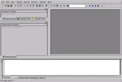
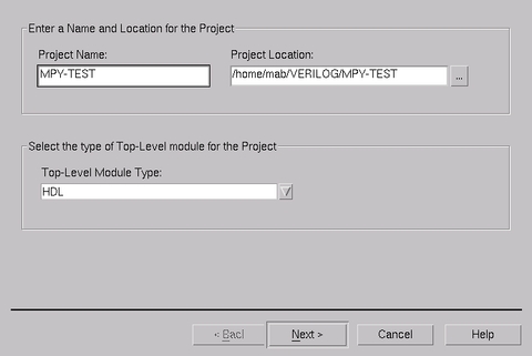
After the software is installed, we open a shell and begin. The process starts by typing ise at the command line. This brings up the Project Navigator, which is the screen shown in Figure 2. To start a new FPGA design project, select a new project under the File menu. This brings up the window shown in Figure 3. Here, we enter a project name, MPY-TEST, and indicate the kind of top-level module we're going to use for this project. We are interested in an HDL top-level module for this tour, but ISE 6.1i allows the use of several other top-level module types.
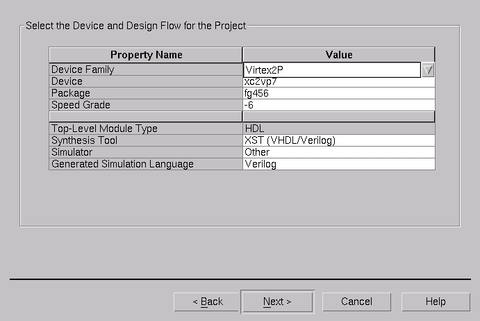
Now that we've selected HDL, the next step is to let the tool know with which kind of FPGA we're going to design. For illustration, we use the most advanced FPGA devices, the Virtex-II Pro family. This is shown in Figure 4, where the xc2vp7 device is selected, along with an fg456 package. This device is one of the smaller Virtex-II Pro parts, but it still has numerous resources. Here, we use only a small part of the device.
The menu window in Figure 4 also allows other choices. You can select the part speed grade, and here we accept the default of -6. The Project Navigator can be used to organize your entire project flow. For instance, you can perform both behavioral simulation and functional simulation. The first type of simulation is a check that you have a logically correct design—that the design does what it's supposed to do. The second type of simulation is post-FPGA implementation, used for design verification of a completed chip. The device selection screen in Figure 4 also includes other options, such as the particular simulator you want to use for HDL simulation and what language to use for simulating an implemented FPGA. This might include, respectively, some industry-standard tools provided by Xilinx partners, or another simulator, and Verilog or VHDL.
Next, we select a new source file for the design and give the design a filename. In this process, we tell the tool what kind of CAD document we're creating; in this case, it's a Verilog module. We enter a filename of mpy16.v, with the .v being the standard filename suffix for Verilog. It is customary, but not required to make the filename for the top-level module the same as the module, or a name like toplevel.v.
Several other kinds of documents can be entered for the tool and added to the project. We don't have time to examine all of these capabilities, which include alternative entry modes (schematics) and the inclusion of standard and custom HDL libraries made by the user.
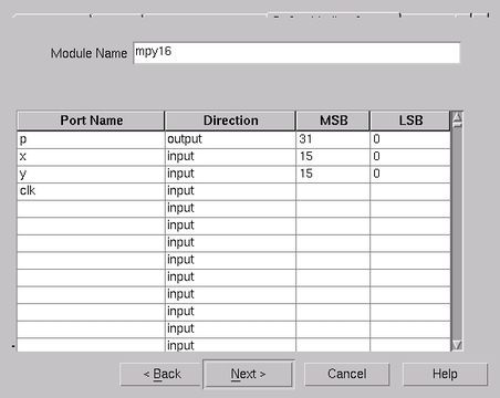
To define this (first) Verilog source for the design, the Design Manager offers some help. For the top-level module mpy16, we fill out a module port table using a tabular entry tool (Figure 5). Here, we define the wires that enter and exit the top-level module, and these will end up as the external I/O pins on the FPGA. The names of the ports entered are p, x, y and clk.
We specify p as a 32-bit-wide output and the main inputs, x and y, as 16-bits wide. Because this multiplier will be pipelined, we also include a port named clk, which will provide the synchronous timing source for the multiplier. The port clk is only a single wire, or net, so we leave out content for MSB or LSB in the table. This means clk will be a scalar. In Verilog, vectors are groups of wires or nets, and these are zero-base indexed.
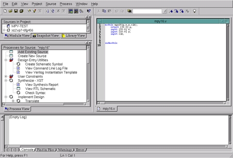
After completing tabular entry for the top-level module, we obtain a summary dialog. Then with the project set up, the Project Navigator brings up all the tools and the initial outline for our Verilog module. This is shown in Figure 6, with the skeleton source code in the upper-right corner. An editor is supplied with ISE 6.1i, and you also can import HDL source code created with the Linux editor of your choice.
Listing 1. The Verilog Source Code for a 16-Bit Pipelined Multiplier
module mpy16(p,x,y,clk);
        output [31:0] p;
        input [15:0] x;
        input [15:0] y;
        input clk;

        // inferable storage via synthesis
        reg [31:0] p;
        reg [15:0] xq;
        reg [15:0] yq;

        // 16x16 unsigned multiplier specified
        // behaviorally
        always @(posedge clk)
                begin
                        xq <= x;
                        yq <= y;
                        p <= xq * yq;
                end
endmodule // mpy16
Listing 1 is the Verilog source code for a 16-bit pipelined multiplier. This code is done in a behavioral style, and we're going to allow Xilinx Synthesis Technology (XST) to figure how to implement what we mean by the code. Today, synthesis is very powerful, and we simply can infer the multiplier hardware, without having to specify its logic design in detail.
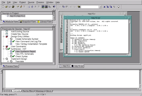
With the Verilog entered, as shown in Listing 1, we start synthesis by double-clicking on the Synthesize - XST button in the Project Navigator tool scroll list. This design we've entered is easy to synthesize and takes only a few moments. The synthesis results can be viewed by reading the synthesis report file (Figure 7). The check marks in the tool scroll list at the left indicate what Project Navigator accomplished. The synthesis report file is in the upper right. You can look through this to see how XST decided to infer your logic to the target FPGA, as well as glean an estimated clock-rate performance for the resulting design in that FPGA.
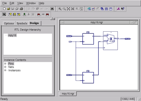
RTL is a view of your logic as various black boxes or logic gates that are situated between flip-flop registers. RTL is the predominant view of logic in synchronous design. The View RTL Schematic button in the ISE 6.1i tools offers an excellent way to get a graphical overview (Figure 8). You can navigate across any hierarchy of modules in your design with the RTL schematic being regenerated dynamically. We're now ready to run the FPGA implementation tools.
We start implementation by clicking Implement Design in the tool list at the left in Project Navigator. For FPGA implementation, the generic process automatically engaged by the tools goes as follows: translate, map and place and route.
In most cases with FPGA design, you do not need to know the specifics of the operation of these steps, with the exception of seeking extremely high performance from the FPGA. But it can be helpful to know what's going on. For example, map determines how the inferred synthesis results get “mapped” to your selected target FPGA. Looking at the map report file can provide useful information about the allocation of resources. Similarly, sometimes it can be useful to read the place and route (PAR) report file to learn whether options are available to improve the speed of your design or to constrain resource utilization more carefully earlier in the toolchain.
Other tools in ISE 6.1i not encountered in this article provide much flexibility for performance engineering and for creating constraints such as locking the FPGA I/O pins for subsequent use with PCB boards, given iterative FPGA implementation to fix bugs.
This design used only one out of the 44 available multipliers on the xc2vp7 FPGA. Also indicated are the 65 I/O pins that were requested for this logic. The Pad report generated by the tool will tell you which FPGA pins were selected in implementation. As mentioned above, you also can preselect these pins for a board design, and this is done with a constraint editor in the tool or by creating a constraint file.
FPGAs are fast CMOS devices. It's important for us to know how fast, in order to verify static timing goals against system requirements. Other important information for system design might include knowing setup time information or clock-to-pin delays. ISE 6.1i provides an integrated timing analyzer. A timing report file can be generated automatically, based on all routing and propagation delays for the completed implementation in the target FPGA.
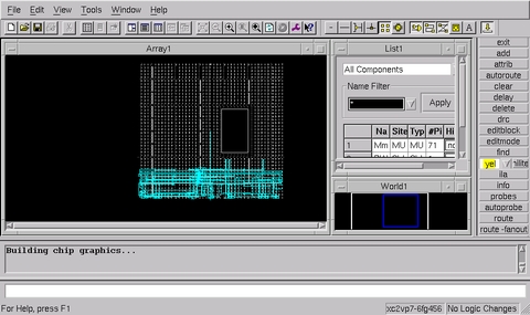
You also can look inside the FPGA device by clicking the FPGA editor tool after implementation. This tool opens a separate screen (Figure 9). The initial view is a called a worldview, where you can see your whole FPGA at once. As you probably can see in the center view, very little of the 2vp7 was used. This view becomes quite dense with high-utilization designs. The large block in the view is the PowerPC microprocessor. Also visible are other multiplier blocks, block RAMs and numerous other elements in the FPGA. Various blocks in the design can be highlighted selectively.
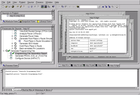
The last step in FPGA implementation is bitgen, or bit generation of the configuration bitstream for the FPGA so that the device can be programmed in a system. After pressing Generate Programming File, the bitstream is created automatically from the FPGA implementation data. The bitgen tool creates a report file, which is shown in Figure 10, in the upper right.
After creating the FPGA bitstream, there are numerous options for using it to create programming files. These depend a lot on the hardware mechanism you want to use for programming the FPGA. The options include PROM file, ACE file, JTAG file and direct configuration of the FPGA.
PROM files are used for conventional PROM programmers, for example, to make an EPROM that goes in your system. ACE files are used with the Xilinx SystemACE CF programming solution. SystemACE CF is a low-cost way to embed a CompactFlash device in your system. Using ACE files, you can create data on a conventional CompactFlash card that can be used for FPGA configuration, dynamic reconfiguration and multiple-device configuration. You also can boot the PowerPC processor this way.
JTAG files are used with Xilinx download cables over a JTAG chain for the FPGA device(s) in your system. JTAG enables configuration, control and bitstream or debugging feedback. In particular, JTAG is the primary mechanism for the Xilinx ChipScope Pro 6.1i tool, which is an integrated logic analyzer that gets embedded into your on-chip logic for live in situ hardware debugging. You also can configure the programming of the FPGA directly from a PC, using the iMPACT tool and a download cable.
The tools also can be used on the command line, instead of with the GUI. Once the Xilinx binaries are on your Linux $PATH, you can drive them with batch mode scripts, programs and makefiles. If you want to run these commands from the shell, you can crib from the command log, produced by the Project Navigator, and improvise from there. For example, these commands can be modified to add shell variables. For the design created in this article, the generated command log text looks like:
xst -intstyle ise -ifn __projnav/mpy16.xst \
-ofn mpy16.syr
ngdbuild -intstyle ise \
-dd /home/mab/VERILOG/MPY-TEST/_ngo -i  \
-p xc2vp7-fg456-6 mpy16.ngc mpy16.ngd
map -intstyle ise -p xc2vp7-fg456-6 -cm area \
-pr b -k 4 -c 100 -tx off \
-o mpy16_map.ncd mpy16.ngd mpy16.pcf
par -w -intstyle ise -ol std -t 1 mpy16_map.ncd \
mpy16.ncd mpy16.pcf
trce -intstyle ise -e 3 -l 3 -xml mpy16 mpy16.ncd \
-o mpy16.twr mpy16.pcf
bitgen -intstyle ise -f mpy16.ut mpy16.ncd
We have introduced FPGAs in the context of modern semiconductor technology, have described how software and hardware lines are blurring and have taken a quick tour of the ISE 6.1i FPGA implementation tools on Linux. You also can refer to the August 2002 issue of LJ (/article/6073), which first introduced the Xilinx ML300 development board and embedded Linux on the Virtex-II Pro FPGA.
Resources
ChipScope Pro: www.xilinx.com/ise/verification/chipscope_pro.htm
Design Tools: www.xilinx.com/ise/design_tools/index.htm
Development and Reference Boards: www.xilinx.com/xlnx/xebiz/board_search.jsp
Embedded Development Kit: www.xilinx.com/ise/embedded/edk.htm
Main Link: www.xilinx.com
Xilinx FPGA Devices: www.xilinx.com/xlnx/xil_prodcat_landingpage.jsp?title=Devices
Useful Verilog Resources
Icarus Verilog: icarus.com/eda/verilog
IEEE Std. 1364-1995 (ISBN 1-55937-727-5): standards.ieee.org
IEEE Std. 1364-2001 (ISBN 0-7981-280606): standards.ieee.org
Verilog Quickstart, Third Edition, by James M. Lee, Kluwer Academic Publishers, 2002. ISBN 0-7923-7672-2.
Verilog is a registered trademark of Cadence Design Systems, Inc.
Michael Baxter is technical editor of Linux Journal.


