Arduino Teaches Old Coder New Tricks
I became aware of the Arduino Project from occasional media reports and a presentation at Atlanta LinuxFest 2009. I was impressed with what the Arduino community was doing, but at that time, I saw no personal use for it. It took a grandson who is heavily involved in a high-school competitive robotics program to change things for me. During a 2011 Thanksgiving family gathering, he asked me some questions about robotics-related electronics, and I told him to google Arduino. He did. Arduino ended up on his Christmas list, and Santa delivered.
I would be more helpful in assisting the grandson's Arduino efforts if I understood more about it myself, so I ordered a couple Arduino Nanos and some peripherals, such as rotors, servos, ultrasonic sensors and LCD displays, and dug in. I now had a purpose for using the Arduino and a reason to dust off my soldering iron. I used a breadboard for testing, as shown in Figure 1.
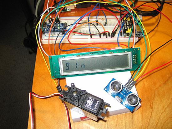
Figure 1. Arduino Pro Mini in Breadboard Tests
It didn't take very long to remove the mental cobwebs and get into the elegant simplicity of the Arduino Project. Years ago, when I built microprocessor projects, the underlying system code always was the problem. Before I actually could write my application, I had to develop or adapt systems-level code to interface the application-level code with the underlying hardware. It was always a major pain and, quite frankly, drudgery. The Arduino Project does away with worrying about most of the low-level systems code, leaving you with the now much-simplified task of creating your application. Using the Arduino IDE and included or contributed libraries enables you to interface to a plethora of hardware easily. Anyone who has developed in the C and C++ languages will find the Arduino platform easy to master quickly. Although Arduino is actually based upon the Wiring Project, compatibility with C, C++ and Linux are very high.
After implementing and testing code for the various peripherals that I had accumulated and generally mastering the Arduino platform, I said to myself, "now what?" So, I abandoned the nice Arduino IDE and switched over to developing code using Linux tools, such as Make. I also wanted to get closer to the hardware, so I abandoned the Arduino boards and did my implementations on the underlying ICs used by all Arduino boards, the Atmel 8-bit series of microcontrollers. Using the Arduino libraries with the Atmel microcontrollers is a joy to behold. I am so thrilled that the drudgery of systems code can be mostly ignored as it is mainly handled by the hardware abstraction features of Arduino's built-in libraries. It is important to note that the Atmel ICs are microcontrollers, not microprocessors. In other words, they are almost complete computers equipped with RAM, EPROM and FLASH memory, multidirectional I/O, serial ports (in some cases) and interface circuitry (such as pull-up resistors and so on). Just adding a power source will yield a computer in a chip.
The hardware's interfaces of the Atmel microcontroller are abstracted by Arduino in a uniform way—at least, uniform for those Atmel micrcontrollers implemented by the Arduino group. Arduino libraries use internal code, generically called the "core", to define the available I/O pins on a given Atmel microcontroller, assigned by pin number. For example, the Atmel ATMega168 physical pin 4 is defined as Arduino I/O pin 2, yet with the Atmal ATMega32u4 microcontroller, the same Arduino pin 2 is matched to physical pin 19. Thus, the Arduino syntax of "pinMode(2, OUTPUT)" defines, in software, an abstracted hardware pin as a digital output. Because the Arduino module pins are labeled with Arduino pin numbers, the abstraction becomes physical, at least on the module level. Nonetheless, it is this abstraction as well as robust libraries that enable the Arduino to be so easy to work with. One caveat alluded to above is that Atmel microcontrollers not implemented in Arduino modules don't have uniform core definitions—for example, the Atmel Attiny series. You still can use the Arduino libraries and tools, but the cores must be obtained elsewhere. For the Atmel ATtiny85 and Attiny 84 microcontrollers, I use the core from the code.google project named arduino-tiny. However, there are other, competing cores around for these chips, and they are not necessarily compatible.
Burning your program into an Arduino module is extremely easy to accomplish. The USB connection not only can power the module as well as serve as the serial communications interface, but the Arduino IDE also uses it to install your program into the Flash memory. It is more complex with the Atmel ATtiny series, because they have no USB port or even a hardware serial port, for that matter. For the ATtiny series, you must use an external programmer. Many people use an Arduino board as the programmer once they have loaded the ArduinoISP software, or sketch, as programs are named in the Arduino world. In my case, I chose to use a dedicated programmer called a USBasp. It is readily available on eBay, or you even can make your own with plans from its creator, Thomas Fischl. I purchased mine on eBay because it was cheaper than the parts cost to make my own. The USBasp uses the open-source AVRdude software.
The Project
Now that I had invested a lot of time into learning the Arduino system and the Atmel microcontrollers, I wanted to take the next logical step: move a design from the breadboard to a printed circuit board. Some interesting projects exist in this area, such as Fritzing, which is designed to facilitate doing exactly that. It's a clever project and you should check it out, but I took a different path—using the gEDA open-source Linux software suite for printed circuit development.
I looked at my inventory of parts and started thinking of what I could create that wasn't already readily available. I settled upon the LCD display. The displays being used in Arduino projects were interfaced with a lot of I/O pins and code space, neither of which are in great supply on the Atmel chips. I felt that if I could create a same-size daughter board that I could attach onto the back of the display and put the smarts into the board that would communicate with the LCD display via an ASCII serial interface, I would have something useful that didn't exist in the marketplace in an affordable form. This is commonly called a serial LCD.
Being somewhat of an old-timer, I spent a lot of time using and coding for the DEC VT100 display terminals upon which the ECMA-48/ANSI X3.64 standards are based. I felt that if I coded the daughter board to turn an LCD display into a tiny, affordable DEC-VT100, I would have something reasonably unique and useful. Serial-driven LCD displays do exist, but they typically have proprietary protocols, and some are rather expensive. As far as I have been able to determine, there exists no open-source (software and hardware) serial LCD display with VT100 protocol. I found my project!
Gathering the Parts
I selected parts for the VT100-LCD project, such that the parts would be as affordable as possible. In fact, I purchased all the parts from two sources, eBay and Digi-Key, based on cost. Table 1 shows the required materials to build one vt100lcd. Costs are shown on a per-item basis; however, I purchased most of these items in quantities of five or more.
| Part | Qty | Source | Cost |
|---|---|---|---|
| 1602 HD44780 LCD | 1 | eBay seller (China) | $2.95 |
| Atmel ATtiny84 | 1 | Digi-Key ATTINY84-20PU-ND | $3.01 |
| Switch, tactile FSM4JH | 1 | Digi-Key 450-1650-ND | $0.80 |
| Socket, IC, 14-pin | 1 | eBay seller (USA) | $0.15 |
| Header, 1X20, Female, 2.54mm | 1 | eBay seller (China) | $0.39 |
| Header, 1X40, Male, 2.54mm | 1 | eBay seller (China) | $0.20 |
| Resistor, 330 ohm, 1/4W | 1 | eBay seller (Thailand) | $0.02 |
| Resistor, 10k ohm, 1/4W | 1 | eBay seller (Hong Kong) | $0.02 |
| Pot, trim, 5k, RM-065 | 1 | eBay seller (USA) | $0.30 |
| Capacitor, .1uf, ceramic disc, 50V | 1 | eBay seller (Hong Kong) | $0.05 |
| Transistor, 2N3906 | 1 | eBay seller (Thailand) | $.01 |
| Diode, 1N4148 | 1 | eBay seller (Thailand) | $.01 |
| Total: | $7.91 | ||
| Optional Parts | |||
| Commercial PCB | 1 | Panel Aggregator | $7.43 |
| Capacitor, 22pf, ceramic disc, 50V | 2 | eBay seller (USA) | $0.40 |
| Crystal, 20MHz, ATS200-E | 1 | Digi-Key CTX1105-ND | $0.64 |
Schematic Design
To design the circuitry for the VT100-LCD, I chose gschem of the gEDA Project by https://geda-project.org. This suite includes not only the schematic design program but also a PCB layout program, as well as various helper programs. A number of schematic/PCB design software programs exist, but I'm focusing on the open-source software of the gEDA Project by geda-project.org here. Other open-source projects that run on Linux, include KiCad, as well as several commercial products, the most popular of which is Eagle PCB by CadSoft, which runs pretty well under WINE.
gschem is fairly straightforward, and many functions are intuitive, but a few, useful but arcane commands necessitate printing out a cheat sheet (hey, I'm getting older and I can't memorize all of those keystrokes). Yes, although gschem is a GUI program, useful keyboard shortcuts appear nowhere in the GUI's menus. This is especially true of the PCB layout program that I discuss later.
The process consists of inserting electronic component symbols into the schematic drawing either from the built-in library or from your private library and then connecting the pins by drawing traces. I highly recommend reviewing the gEDA Project's on-line documentation before starting your own schematic. There are a few tutorials on the Web about using the gEDA suite, and Stuart Brorson wrote a tutorial article in the November 2005 issue of Linux Journal (see Resources).
I created two versions of my VT100-LCD project: one using the eight-pin ATtiny85 microcontroller and another using the 14-pin ATtiny84 microcontroller. The schematic for the ATtiny84 microcontroller version is shown in Figure 2.
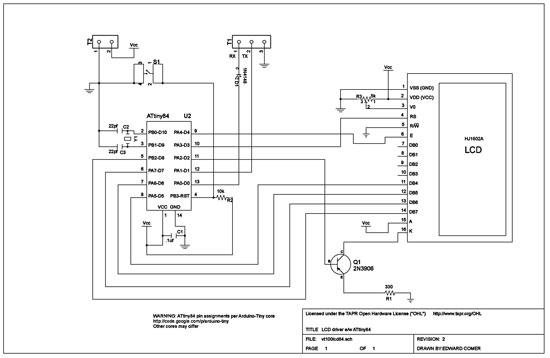
Figure 2. Schematic for VT100LCD e/w ATtiny84
Because some of the components I was using do not exist in the built-in library, I scoured the Internet for contributed symbols, and in a few cases, I had to design my own symbols. A good source for contributed symbols and footprints is https://gedasymbols.org. For creating your own symbols, see David Weber's Online Symbol Creation Tool at https://EmbeddedToolBox.com. Symbols actually are text files. Figure 3 illustrates a symbol along with a portion of the text file used to draw it. Symbol files are not just an image. They also hold important pin definitions and the name of the footprint file that the gEDA PCB program ultimately will use to represent the component on the circuit board.
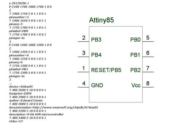
Figure 3. Symbol Example 1
A gEDA schematic is a text file interpreted for GUI presentation by gschem, but it also serves as the source for gEDA's PCB program. An intermediary helper program named gsch2pcb is used to prepare the schematic file for use as input to the PCB program. While xgsch2pcb is a GUI version of gsch2pcb for gsch2pcb, I use the gsch2pcb command-line version. For example, given the schematic file vt100lcd84.sch as an input, gsch2pcb creates vt100lcd84.pcb, vt100lcd84.net and vt100lcd84.cmd, all necessary files for PCB creation. gsch2pcb also displays important instructions as part of its command-line text output. To make the process a little easier, I use a file named "project" in the project folder for the current design. Figure 4 shows my project folder for the vt100lcd84 project, the "project" file and the command line with the gsch2pcb command just before execution.
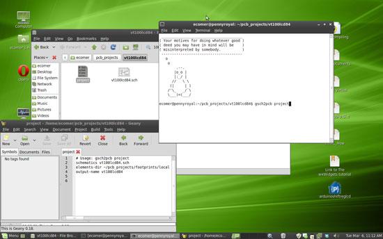
Figure 4. Example of gsch2pcb Project File
It is worth noting that the gEDA suite includes circuit simulation capability (SPICE), enabling virtual design testing. I did not use SPICE with my VT100-LCD project, but see the Resources for this article if you are interested.
Software Design
Now that I had the circuitry designed for the project, it was time for the software. I wrote the software as a simple state machine that parses each character received on a character-by-character basis, meaning that there is no buffer. Characters are handled differently based upon the current state of the machine. If the state is NOTSPECIAL, the character simply is passed to the LCD screen for display. However, if the state is GOTESCAPE, GOTBRACKET or INNUM, the character is processed further. For example, if the state is GOTBRACKET, both an escape and left-bracket character have been received previously, and the current character must be parsed in that context. For illustration, the VT100 sequence for Screen-Clear is \033[2J, and if the current character being parsed was the 2, the state would be GOTBRACKET, and the next state would be INNUM (number collection).
This method of parsing has the advantage of simplicity, which is suitable for the limited-capacity microcontrollers but with the disadvantage of not being able to scroll the screen due to the absence of a buffer holding a copy what is on the screen. See Resources for a copy of the software source. I used Arduino libraries to build the code. Although the source can be compiled using the Arduino IDE, I used Linux make. Using the Arduino libraries makes the project extremely easy to build. Most of the drudgery of low-level code and the bootloader is hidden away within the Arduino libraries, which freed me to focus solely on my project. Even main() is hidden away such that Arduino code contains two required routines: setup() and loop(). Main actually does exist deep in the Arduino directory structure in ~/arduino/arduino-1.0/hardware/arduino/cores/arduino/main.cpp and is automatically linked in at compile time.
| Return | Cursor to leftmost of current line |
| Linefeed | Cursor down |
| Esc c | Resets LCD |
| Esc D | Cursor down |
| Esc M | Cursor up |
| Esc E | Move cursor to start of next line |
| Esc [ A | Cursor up one line (arrow key) |
| Esc [ B | Cursor down one line (arrow key) |
| Esc [ C | Cursor right one column (arrow key) |
| Esc [ D | Cursor left one column (arrow key) |
| Esc [ H | Cursor to HOME 1;1 |
| Esc [ s | Save cursor position |
| Esc [ u | Restore to saved cursor position |
| Esc [ m | All attributes off |
| Esc [ Pn A | Cursor up Pn lines |
| Esc [ Pn F | Cursor up to column 1 of Pn lines |
| Esc [ Pn B | Cursor down Pn lines |
| Esc [ Pn E | Cursor down column 1 of Pn lines |
| Esc [ Pn C | Cursor right Pn characters |
| Esc [ Pn D | Cursor left Pn characters |
| Esc [ Pn G | Cursor to column Pn of current line |
| Esc [ 2 J | Erase Screen and home cursor |
| Esc [ P1;PcH | Direct cursor addressing, where P1 is line# |
| Esc [ P1;Pcf | Same as above |
| Esc [ = Pn h | Set (LCD lines) - Pn 2 = 16X2 - 4 = 16X4 |
| Esc [ 0 m | All attributes off (underscore cursor off) |
| Esc [ 4 m | Underscore on |
| Esc [ 0 c | Report terminal type |
| Esc [ 5 n | Reports max qty lcd lines (1s based) |
| Esc [ 6 n | Reports cursor position (1s based) |
| Esc [ 0 q | Turn LCD's LED 1 off |
| Esc [ 1 q | Turn LCD's LED 1 on |
PCB Layout
When the .pcb file is opened with gEDA's PCB program and the commands invoked are listed in the gsch2pcb command-line text output, you are presented with a jumble of components. I first dispersed the components manually with an approximate placement and then activated the "rats-nest" display. The "rats-nest" is the connections that must be converted to copper traces. After shifting around components to visually bring the "rats-nest" connections to their shortest routes, I was presented with what you see in Figure 5.
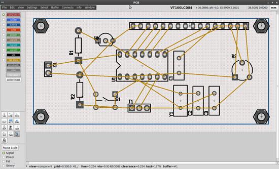
Figure 5. Components with Associated Rats-Nest
PCB possesses the ability to auto-route the traces, namely convert the "rats-nest" into copper trace representations. This tends to do some odd things but produces a workable PCB design once a cleanup is done. I chose a semi-manual layout so I could control the placement and appearance. Basically, I used the auto-route for the power traces, did some manual cleanup, then used auto-route for the signal traces, followed by more cleanup. The result was similar to Figure 6, which is my second and final version of the layout for the ATtiny84 version of my VT100LCD project. PCB Manufacture Printed Circuit Board layout consists of applying upon a copper laminated board an acid-resistant pattern that represents the areas that are to retain copper after etching in an acid solution (etchant). Areas of the copper laminated board that are exposed to the etchant will be dissolved away, leaving the areas under the acid-resistant pattern intact.
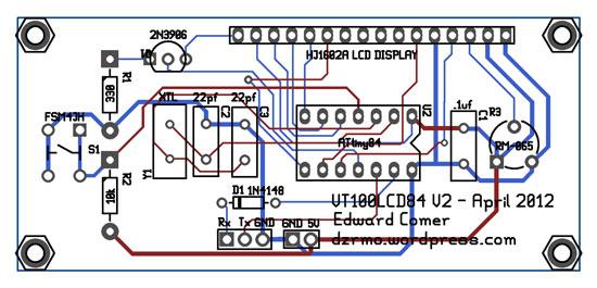
Figure 6. Final Layout of vt1001cd84 Project
Years ago, I occasionally used to make Printed Circuit Boards using a photographic method that is less common in the DIY community today. The acid-resistant pattern was laid out by hand onto translucent or clear drafting paper using fine black tape for circuit paths and dry transfer patterns for components. This pattern is typically a positive, similar to Figure 7, so a negative must be made photographically for the process to work. The end result is that the negative's acetate sheet is clear where copper should remain after etching. This photographic work formerly was done in a darkroom, but today, creating the negative can be done using a computer printing to a transparency sheet. I don't discuss the process here, but an example is shown in Figure 8.
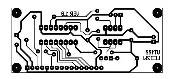
Figure 7. Layout Positive
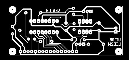 d/u1002061/11300f8.jpg" alt="" title="" class="imagecache-large-550px-centered" />
Figure 8. Layout Negative
Next, the prepared negative pattern would be affixed on a copper laminated board that has a light-sensitive diazo-type emulsion as a top layer. Exposing the prepared PCB to ultra-violet light would alter the properties of the exposed (clear) areas that received the ultra-violet light. Washing the exposed board in a chemical developer dissolved the exposed portions of the emulsion, leaving intact the emulsion that was under the black portions of pattern on prepared negative sheet. Many commercial systems still do a modernized variation of this process as do some serious DIYers.
The casual DIY community has, thankfully, adopted a new and much easier method of PCB layout for medium-density layouts. High-density layouts still should use the photographic process. The new DIY PCB layout process is commonly called the toner transfer method, because a laser printer is involved. Thankfully, the old paste-up tape and dry-transfer component patterns are a thing of the past. Computer software is now available for the DIY community that takes software-designed schematics as input and produces a representative PCB layout (Figure 7 was produced by such software).
As I mentioned earlier, a number of PCB design software programs exist, but I'm focusing on the open-source PCB program of the gEDA project by geda-project.org here. An example of an in-progress gEDA PCB layout is shown in Figure 9, and its final output is a positive similar to Figure 7.
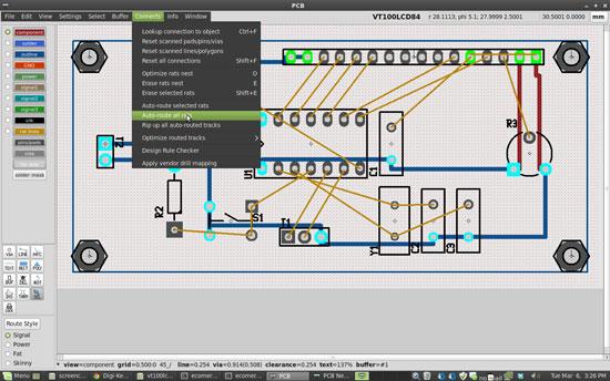
Figure 9. gEDA PCB Layout in Progress
The positive of Figure 7 needs to be printed in reverse onto a paper that easily will release the toner when heated. Laser printer toner is a finely ground polymer plastic that is fused to the paper by heat. The trick of the "toner method" is to get the toner to transfer from the paper to the copper-laminated board once it is re-heated. A big part of the secret here is the type of paper you use.
Several paper solutions for the "toner method" exist, and some are better than others. Regardless of the type of paper used, the process is to place the reverse image positive laser print with the toner touching the metal surface of a clean copper-laminated board and then apply heat and pressure to loosen the toner from the paper, permitting it to transfer to and adhere to the copper laminated board. Most DIYers use a common clothes iron as the heat source, although a laminating machine designed for identification cards is successfully used with one commercial product that I'll talk about later.
The cheapest and simplest method is simply to use ordinary copier paper. Once heated under pressure, the toner ends up adhering to both the paper and the copper-laminated board. The paper/copper-laminated board is then soaked under water, and the waterlogged paper is rubbed off with your fingers. This method leaves a lot of paper residue embedded in the toner's surface, this is undesirable for reasons explained later.
Many other paper types are used by various DIYers. One of the most popular is to use a high-quality magazine page that has a smooth, glossy appearance. The gloss is caused by a white clay (kaolin) coating. Because the kaolin fills in many of the pores of the paper, the toner is less firmly bonded to the paper. Second, the kaolin dissolves in water, thus freeing the toner more readily than plain paper. This method is superior to using plain paper, but it still leaves too much paper residue embedded in the toner's surface.
Another popular method is to print onto the glossy side of photo paper or backing paper for labels. This method is superior to either plain paper or high-quality magazine paper, because there is no paper residue embedded in the toner's surface. However, a significant problem with this method is actually getting the toner to stick to the paper evenly. Quite often, PCB traces simply fall off the slick surface while the paper works its way through the printer. Obviously, there is a lot of variability among laser printers and glossy paper types. I don't like variability; I like dependable repeatability.
This leads me to the paper and method I use that has dependable, predictable results. The paper is colloquially known as dextrin-coated paper. Some DIYers actually make their own by making dextrin and coat paper with it. Dextrin is simply cooked corn starch, and the process is easy albeit a bit labor- and time-intensive. Also, getting an even coat is a challenge. If you are interested, numerous articles and videos exist on the subject—simply google "make dextrin paper". I, however, feel that purchasing commercial dextrin paper is worth the cost. My preferred product is made by PulsarProFX (https://www.pcbfx.com). The company primarily sells a kit called Fab-In-A-Box, but the entire kit isn't really necessary. Instead, buy the refill package of Transfer Paper. Also buy the Green Toner Foil. Digi-Key sells refill kits of both. Pulsar really pushes use of a laminator but cautions that its laminator isn't hot enough to melt the toner used in Brother laser printers. My printer is a Brother HL-2140, so I simply use a clothes iron. A word of caution here: use genuine Brother toner. After-market toner cartridges may contain fuser oil that prevents the toner from adhering to copper. After several failed boards, I figured out that the problem was my new Rosewill-brand toner cartridge. When I put in a genuine Brother cartridge, my boards were successful again.
You need the Green Toner Foil because the toner adhering to the copper-laminated board is porous, and even though you cannot see it with the naked eye, there are sufficient holes for the etchant to penetrate the toner traces and remove metal that you do not want removed. The Green Toner Foil is ironed onto the copper-laminated board resident toner, creating a smooth, impervious surface on the top of the toner traces, resulting in superior board etches. Now, remember that I said that the aforementioned transfer methods were deficient due to paper residue embedded in the toner's surface? This is because the paper residue prevents the Green Toner Foil from making a good bond to the toner.
How do I make my own single-sided PCBs? It's fairly simple:
-
Print a reverse image positive of the PCB pattern onto the shiny side of Pulsar dextrin transfer paper.
-
Place the transfer paper's toner side against a copper-laminate board that has been cleaned with steel wool.
-
Place a sheet of ordinary paper above the transfer paper to help prevent slippage.
-
For two minutes, apply, with a few of pounds of pressure, a common clothes iron set to the highest "cotton" setting.
-
Immerse into water, the ironed-together paper/copper-laminate board. After a couple minutes, the paper probably will float off. If it doesn't, lift it off.
-
Dry the board, and with the toner side up, lay the dull side of the Green Toner Foil against the toner and another piece of ordinary paper above that.
-
Using the same clothes iron set slightly cooler (to "wool"), iron for one minute with a few pounds of pressure.
-
Peel off the Green Toner Foil.
-
Etch the board as described below.
I make only single-sided boards. If you'd like to make a double-sided board, watch the video at https://youtu.be/XX7IekbCNIY. This DIYer uses HP's glossy brochure paper and seems to get pretty good results.
Etching the PCB
Having read much of what is readily available on the Web concerning DIY PCB etching, when the need arose, I decided to etch a single-sided board two different ways: first with the vinegar and salt method and second with the sponge and ferric chloride method. Some DIYers are using muriatic acid, but I have not tried that.
The vinegar and salt method works, albeit slowly. Etching my small board took two hours. The formula I used was equal parts vinegar and hydrogen peroxide and a few tablespoons of table salt. Keep adding salt until the "fizzing" continues all by itself. The liquid starts out clear but then turns an attractive shade of blue (Figure 10).
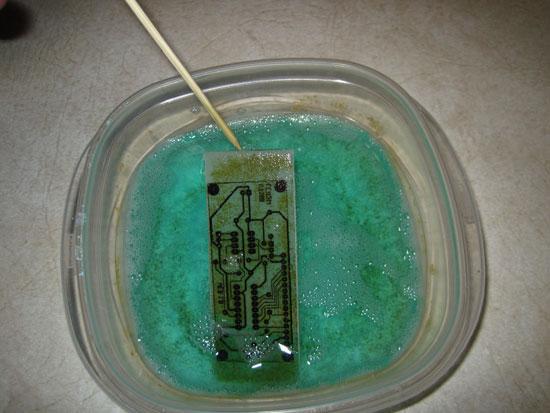
Figure 10. Vinegar and Salt Etchant
The sponge and ferric chloride method works extremely well, etching the same board in a couple of minutes. In the past, I used ferric chloride to etch boards by placing them into a bath of ferric chloride. Even with agitation, etching a board could take ten minutes or so. The sponge and ferric chloride method accelerates the etching by continuously rubbing the surface with a sponge soaked in ferric chloride. The rubbing removes the oxide layer that continuously builds up, permitting the ferric chloride to get to the raw metal and thus accelerate etching. Instead of a tub of etchant, a couple tablespoons is all you need, which will make a bottle of ferric chloride last for a very, very long time. The technique is simple. Don plastic gloves, pour a couple tablespoons of ferric chloride into a small container, soak a small piece of soft sponge in the ferric chloride, then continuously and lightly rub the saturated sponge on the PCB. In a couple minutes, the board will be finished with little mess and little ferric chloride to dispose of.
My final product (after three versions), a single-sided ATtiny84 version of the project, is shown in Figure 11. Given that the board was single-sided, nine jumpers were required, which are the wires you can see on the component side of the board.
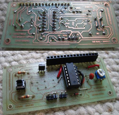
Figure 11. Final Etched ATtiny 84 Board
Commercially Made PCBs
In addition to making my own PCBs, I also had commercial boards made by a panel aggregator. A panel aggregator is a service that aggregates boards from many sources, filling up a cost-efficient-size printed circuit board panel and then breaking up the completed panel for delivery. Several such companies support the hobbyist community.
Figure 12 shows my Attiny85 design mounted to a 16x2 LCD.
Figure 13 shows my Attiny84 design mounted to a 16x4 LCD.
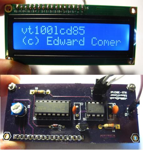
Figure 12. Commercially Made ATtiny85 Board
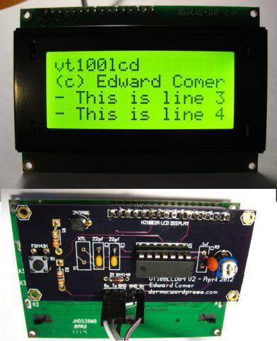
Figure 13. Commercially Made ATtiny84 Board
Resources
Source Code and Hardware Files for the vt100lcd (interested readers can pull down the files and create their own micro-terminal): https://code.google.com
The Arduino Project: https://arduino.cc
The Wiring Project: https://wiring.org.co
The code.google arduino-tiny Project: https://code.google.com/p/arduino-tiny
Thomas Fischl's USBasp Web Site: https://www.fischl.de/usbasp
Avrdude Device Programming Software: https://www.nongnu.org/avrdude
The Fritzing Project: https://fritzing.org
The gEDA PCB Development Project: https://www.geda-project.org
Symbol Creation: https://embeddedtoolbox.com/mksym
Footprint Creation by Stefan Salewski: https://www.ssalewski.de/SFG.html.en
"Circuit Design on Your Linux Box Using gEDA" by Stuart Brorson, Linux Journal November 2005: https://www.linuxjournal.com/article/8438
Using gEDA, by Iznogood: https://www.linuxfocus.org/English/December2004/article355.shtml
Getting Started with PCB: https://www.delorie.com/pcb/docs/gs/gs.html
gsch2pcb Tutorial: https://geda.seul.org/wiki/geda:gsch2pcb_tutorial
gschem → gsch2pcb → PCB: https://tinyurl.com/gsched2pcb
Circuit Simulation using gEDA and SPICE—HOWTO by Stuart Brorson: https://www.brorson.com/gEDA/SPICE/intro.html


